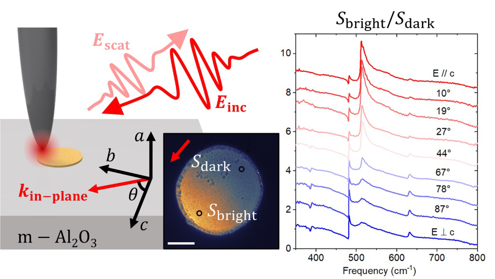
Infrared light has the right energy range to probe many interesting material properties, including the vibrational modes of molecules and the way electrons interact with external photons. As devices get smaller and faster, the ability to study the way light and matter interact at the nanoscale will become crucial for the development of quantum and microelectronic technologies.
A powerful infrared method for probing such phenomena is called scattering-type scanning near-field optical microscopy (s-SNOM), which uses the tip of an atomic force microscope (AFM) to focus infrared light down to about 10 nm, below the wavelength of the light itself (i.e., below the diffraction limit). However, because of the elongated geometry of the AFM tip, oriented perpendicular to the sample, s-SNOM is less sensitive to features of interest that lie parallel to the sample surface.
“Probing in-plane responses at the subwavelength scale has been a long-time hurdle for the technique,” said Ziheng Yao, a former ALS doctoral fellow and co-first author of a Nature Communications paper that reports on a way around this hurdle. “With our results, we can get not only the the top view of the object, but also the side views.”
At ALS Beamline 2.4, the researchers used s-SNOM to study samples of sapphire and LiNbO3, two well-characterized, prototypical materials suitable for a proof-of-concept demonstration. Both have a property (the dielectric function) that varies along different in-plane crystal axes.
On each sample, the researchers fabricated a micron-sized gold disk that acts as an “antenna,” converting the in-plane substrate dielectric response to an out-of-plane field intensity and phase contrast, which can be readily measured by s-SNOM infrared nanospectroscopy.
By measuring the resonance of the fabricated gold disk and comparing the spectra at two “hot spots,” the in-plane response of the sample can be mapped out. Because the gold disk is a subwavelength structure, the spatial resolution remains below the diffraction limit.
The method is a step toward more quantitative measurements with s-SNOM, and will be beneficial for characterizing the in-plane nanoscale properties of objects such as van der Waals materials, microcrystals, topological insulators, or multilayered samples.

Z. Yao, X. Chen, L. Wehmeier, S. Xu, Y. Shao, Z. Zeng, F. Liu, A. McLeod, S. Gilbert Corder, M. Tsuneto, W. Shi, Z. Wang, W. Zheng, H. Bechtel, G.L. Carr, M. Martin, A. Zettl, D. Basov, X. Chen, L. Eng, S.C. Kehr, and M. Liu, “Probing subwavelength in-plane anisotropy with antenna-assisted infrared nano-spectroscopy,” Nat. Commun. 12, 2649 (2021), doi:10.1038/s41467-021-22844-3.