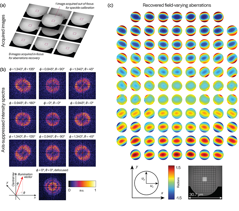
To see clearly at the nanometer scale, scientists must measure aberrations in the lenses used to focus x-ray light, just as optometrists must determine the proper lens prescription to correct a patient’s eyesight. Although many aberration-measurement techniques exist for visible-light optics, they can be difficult or impractical to apply at x-ray or extreme ultraviolet (EUV) beamlines.
Here, researchers developed an in situ computational technique for measuring aberrations, using the SHARP extreme ultraviolet (EUV) microscope at ALS Beamline 11.3.2. Semiconductor industry collaborators use SHARP as a test bed for current and future EUV lithography methods for manufacturing the photomasks used to transfer circuit patterns onto chips.
While photomasks are polished to nanometer-scale smoothness, a small amount of residual roughness provides enough information to decipher aberrations. The large bandwidth and statistical uniformity of their natural surface roughness make them ideal for probing system characteristics, eliminating the need for custom test objects, which are inherently difficult to manufacture.
The new method requires only ten images of a photomask surface, acquired under steerable, coherent illumination, to achieve a measurement accuracy better than 1/180th of SHARP’s 13.5 nm wavelength, or 0.75 Å. The experiments confirmed SHARP’s diffraction-limited performance and affirmed its value as a photomask imaging tool.
Overall, the work demonstrates the value of speckle imaging for characterizing and aligning coherent beamlines. As x-ray light sources progress toward diffraction-limited storage rings, this versatile, in situ technique will prove increasingly valuable in the characterization of coherent sources and beamline optical systems.

G. Gunjala, A. Wojdyla, S. Sherwin, A. Shanker, M.P. Benk, K.A. Goldberg, P.P. Naulleau, and L. Waller, “Extreme ultraviolet microscope characterization using photomask surface roughness,” Sci. Rep. 10, 11673 (2020), doi:10.1038/s41598-020-68588-w.