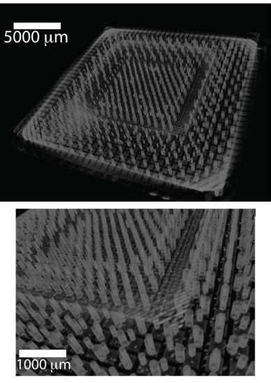
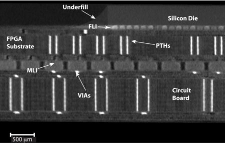
Intel, the world’s largest semiconductor chip maker and inventor of the microprocessors found in most personal computers, is constantly striving to keep products at the technological cutting edge. To further that goal, the company has been using the tomography capabilities at ALS Beamline 8.3.2 to image their microelectronic packages in 3D at high resolution with short throughput time. This research has provided Intel with valuable information for both failure analysis and product development and has proven to the industry as a whole that synchrotrons are an insightful tool for this type of imaging.
A microelectronic package consists of a silicon chip integrated through various components into a protective enclosure that can then be placed into a device—a computer, cell phone, or other electronics. The “package” itself can be composed of various materials and components and is extremely small—the ones that Intel has been imaging at the ALS are about 6 mm, and the features inside the package are even tinier, some as small as 15 μm. Due to the complexity of these packages, multiple points of failure may exist in different locations in a package following a reliability test, thus non-destructive failure-analysis techniques with shorter throughput times are highly desirable. However, performing failure analysis at this level is challenging, especially when many microelectronic packages contain multiple levels of high-density interconnections. Failure can be the result of thermal, mechanical, or electrical stress and can affect performance and sometimes overall life expectancy of an electronic device.

With packages growing ever-more complex, the microelectronic industry is in need of a solution for high-resolution, non-destructive imaging for failure analysis, quality control, reliability risk assessment, and development, says Yan Li, a packaging engineer at Intel who conducted research at Beamline 8.3.2 in collaboration with Lawrence Livermore National Laboratory Materials Scientists Holly Carlton and John Elmer. Certain defects, such as voids and cracks that form inside copper substrate and voids in solder joints, require a technique that can detect features less than 5 µm in size. During the substrate assembly process these types of defects must be identified and monitored extensively to avoid failures.
“This research group from Intel does a lot of characterization, but had never done so at a synchrotron,” says Carlton, who worked closely with Intel on this research. “This was a proof-of-concept type of project, and I was really impressed that three publications resulted from this collaboration.”
The microtomography capabilities at Beamline 8.3.2 allowed the researchers to image an entire microelectronic package with a cross-sectional area of 16 x 16 mm in just three minutes with an 8.7 µm spatial resolution. In contrast, a conventional computed tomography system would take hours to record data with potentially poorer resolution, says Carlton. “The main advantage to imaging at a synchrotron is the reduction in throughput time, which we achieved using a setup that ALS Beamline Scientist Dula Parkinson helped us optimize,” says Elmer. Intel has been able to quickly image packages in 3D at the ALS and identify failures in packages during thermal, electrical, and mechanical stressing of components.

“We showed the industry that this is a successful way to image microelectronic packages with a very fast throughput time,” says Carlton.
“People have been really interested in our research because the results obtained at the ALS suggest a path forward for new applications in microelectronic, and also provide directions for next-generation, lab-scale x-ray technology,” says Li. “Intel and the semiconductor industry in general can benefit from this research, as it allows for improvements in microelectronic packaging interconnect quality and reliability monitoring.”
Carlton, Elmer, and Intel made an instructional video together about how to use tomography beamlines to conduct this type of research.
Research conducted by: H.D. Carlton and J.W. Elmer (Lawrence Livermore National Laboratory); Y. Li, M. Pacheco, and D. Goyal (Intel Corporation); and D.Y. Parkinson and A.A. MacDowell (ALS).
Publications about this research: H.D. (Barth) Carlton, J.W. Elmer, Y. Li, M. Pacheco, D. Goyal, D. Y. Parkinson, and A.A. MacDowell, “Using synchrotron radiation micro-tomography to investigate multi-scale three-dimensional microelectronic packages,” J. Vis. Exp. 110, e53683 (2016). doi: 10.3791/53683
J.W. Elmer, Y. Li, H.D. Barth, D.Y. Parkinson, M. Pacheco, and D. Goyal, “Synchrotron radiation micro-tomography for large area 3D imaging of multilevel microelectronic packages,” J. Electron. Mater. 43, 4421 (2014). doi: 10.1007/s11664-014-3375-z
Y. Li, M. Pacheco, D. Goyal, J.W. Elmer, H.D. Barth, and D. Parkinson, “High resolution and fast throughput-time x-ray computed tomography for semiconductor packaging applications,” 64thIEEE ECTC, 1457 (2014). doi: 10.1109/ECTC.2014.6897485
Operation of the ALS is supported by the U.S. Department of Science, Office of Science, Basic Energy Sciences Program.