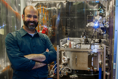
Kenneth Goldberg, deputy director of the Center for X-Ray Optics (CXRO), has been a part of the ALS since 1993, when he began setting up one of the first experiments on the floor, a project in coherent EUV optics. After completing his PhD in physics at Cal in 1997, Goldberg joined CXRO as a staff scientist.
These days, Goldberg’s work is funded by SEMATECH, a consortium of semiconductor manufacturing companies that includes IBM, Intel, GlobalFoundries, and Samsung. SEMATECH, through CXRO, funds several research and engineering projects at ALS beamlines, including Goldberg’s beamline, 11.3.2. CXRO has a long history of collaboration with SEMATECH; CXRO scientists and engineers have built many of the advanced experimental tools for photolithography research that are keys to finding new directions in chip-making technology.
“Semiconductor manufacturers are always looking for ways to make chips that are smaller, faster, cheaper,” says Goldberg. “They follow Moore’s Law.”
What’s helping SEMATECH keep up with Moore’s Law these days is the new extreme-ultraviolet-wavelength microscope, SHARP, that Goldberg’s group commissioned in June 2013. Developed in-house by CXRO scientists, engineers, and technicians, SHARP performs unique measurements for semiconductor manufacturing research, focusing on photomask imaging, a diagnostic tool that is critical for the commercialization of EUV lithography. Photomasks, the glass plates that carry the patterns for each single layer of a computer chip’s circuitry, are extraordinarily complex and even a nanoscale defect can ruin a circuit. SHARP can characterize defects with great detail. Unlike conventional microscopes, electron microscopes, and atomic-force microscopes (AFM), SHARP operates with extreme-ultraviolet (EUV) light, near 13.5-nm wavelength, the same color of light used in next-generation chip-making tools. Beyond that, SHARP provides customizable sample-illumination patterns, referred to as coherence control, that lithographers use to push the physical limits of fine-patterning.
“With these photomasks, there are a lot of open questions,” says Goldberg. “It’s a very complex optical system, with dozens of thin layers and five or more different materials all sitting on an atomically smooth surface. A lot of the research we do helps support the development of the masks—to make the mask work, to make it more efficient, to make it more inspectable, and to validate cleaning and pattern-repair work done at other facilities.”
It’s the depth of experience that’s a unique strength in the CXRO, the group that made the development of SHARP possible, along with the funding from SEMATECH. Regarding the new microscope, Goldberg asked, “How many times in your career do you get to start with a clean sheet of paper and say, ‘How would I do this if I had the chance to do everything right?’”
“I’m really proud that the work we do guides a multi-trillion dollar industry,” he says. “Our research has direct, profound effects on the decisions they make, and eventually the gadgets they produce.”
Even though the semiconductor industry is the second biggest in the U.S., the research teams for these companies can be small, says Goldberg. In EUV it can be just a handful of people, and they rely heavily on the ALS tools to inform them of where to take their products, he says. There are a few other facilities with microscopes that offer semiconductor companies some research capabilities, but none today with the capabilities of SHARP. After less than a year of operations, the data from the SHARP tool is already well represented in papers at the main industry conferences, says Goldberg.
“Making a complex system like that work is one of the most fun aspects of the job,” says Goldberg. “We are continually optimizing SHARP and discovering new capabilities; it’s an ongoing, exciting process.”