A new center, called CHiPPS—or the Center for High Precision Patterning Science—led by Berkeley Lab microelectronics expert Ricardo Ruiz, could accelerate the next revolution in microchips, the tiny silicon components used in everything from smartphones to smart speakers, life-saving medical devices, and electric cars. Read more »
Pushing the Boundaries of Moore’s Law: How Can Extreme UV Light Produce Tiny Microchips?
For the past 25 years, scientists and engineers from the Center for X-Ray Optics (CXRO) have worked to develop EUV lithography, a technique that enables microchip circuits and transistors that are tens of thousands of times thinner than a strand of human hair. Patrick Naulleau, a CXRO scientist who helped develop EUV lithography, shares his perspective in this Q&A. Read more »
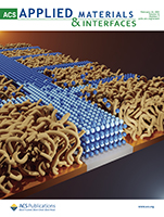
Additive Lithography–Organic Monolayer Patterning Coupled with an Area-Selective Deposition
This scene depicts the layer-by-layer growth of an inorganic film in a selected area. The alternation of a chemical agent (blue) deposits on a gray substrate to form an inorganic film. A cross-linked organic material (tan) locally inhibits this reaction and prevents film deposition. Furthermore, the pattern-wise cross-linking of this organic film enables nanoscale pattern generation. Read more »


