SCIENTIFIC ACHIEVEMENT
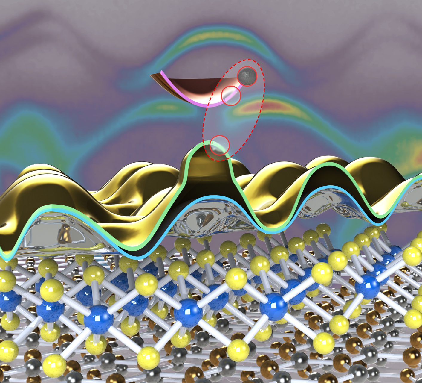
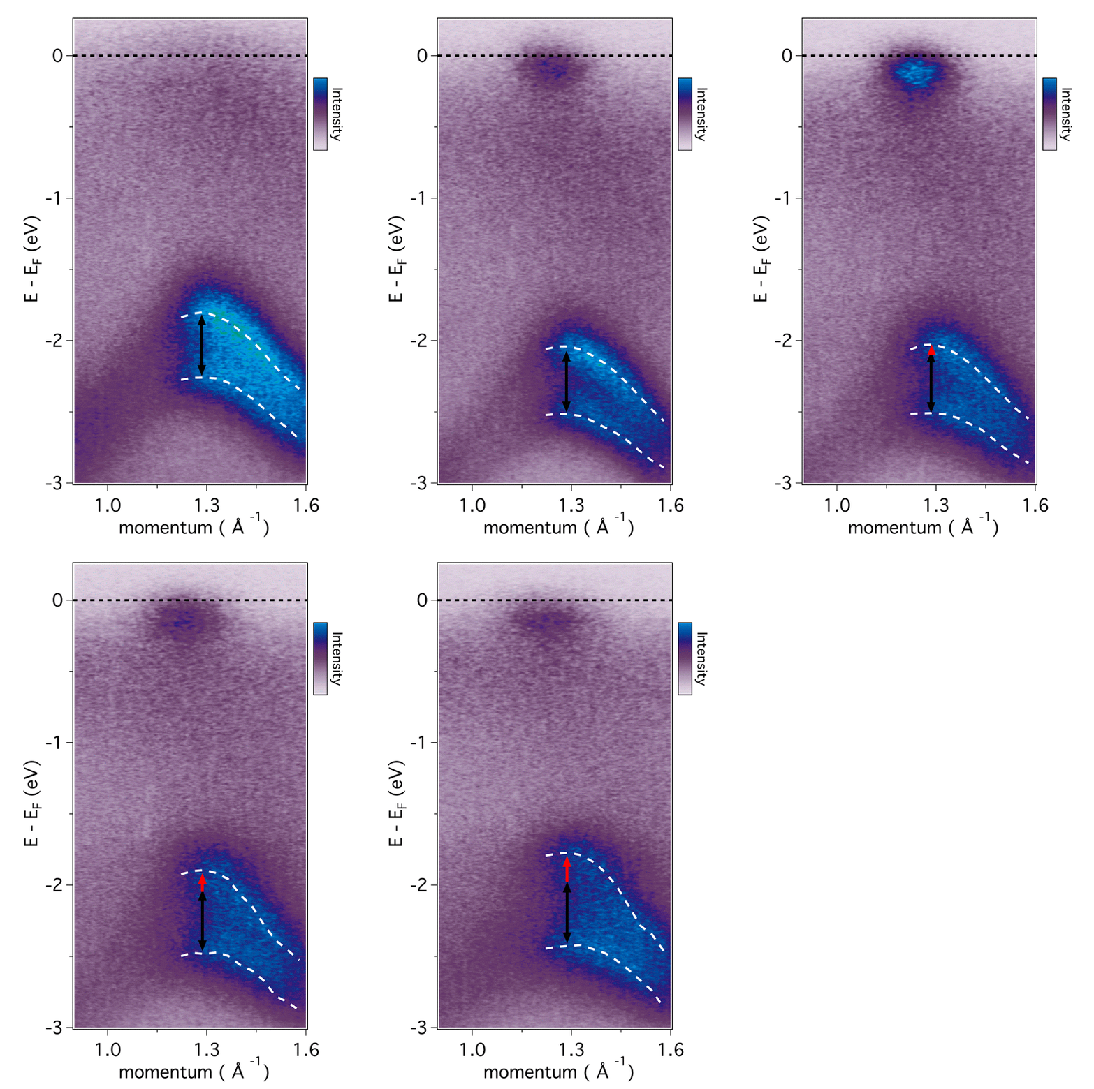
The electronic structure of a stacked 2D material was tuned by in situ electron doping, resulting in a large increase in the splitting of two valence bands.
SIGNIFICANCE AND IMPACT
Stacked 2D materials possess an array of tunable properties that are expected to be important for future applications in electronics and optics.

Mix ‘n’ match materials
When some atomically thin—or 2D—materials are stacked like Lego bricks in different combinations with other ultrathin materials, new properties often emerge that are potentially useful for next-generation device applications. For example, tungsten disulfide (WS2) is a semiconductor that belongs to a family of 2D materials (transition-metal dichalcogenides, or TMDs) that have received an enormous amount of interest due to their many advantageous properties that can be tuned by mixing and matching them in stacks with other 2D materials.
In this work, single-layer WS2 was stacked on a thin flake of hexagonal boron nitride (h-BN), all on a base of titanium dioxide (TiO2). This heterostructure provided a stable, non-interacting platform that enabled a team of researchers to directly and accurately probe the WS2 electronic states and excitations, including the effects of interactions between the electrons themselves (many-body effects), at a level of detail not previously possible.
MAESTRO’s exquisite sensitivity
MAESTRO (Microscopic and Electronic Structure Observatory), a facility at ALS Beamline 7.0.2 that opened to scientists in 2016, can handle very small sample sizes, on the order of tens of microns, which is key to studying 2D materials. Scientists are continuing to push MAESTRO’s capabilities to study even smaller features—down to the nanoscale. The endstation also features the ability to fabricate and manipulate samples for x-ray studies while maintaining pristine conditions that protect them from contamination.
To probe the WS2 electronic structure, the researchers used micro-focused angle-resolved photoemission spectroscopy (microARPES), a technique in which a beam of x-rays, focused to 10 µm, is used to kick electrons out of the sample. By analyzing the ejected electrons’ direction and energy, the researchers can obtain the material’s band structure—a map of the electrons’ behavior in the semiconductor. Moreover, the technique is capable of resolving many-body effects and capturing subtle changes caused by the stacking of 2D materials.
Doping splits up the band

Seeing the intrinsic electronic properties of WS2 was an important step, but the biggest surprise emerged when the researchers increased the number of electrons in the system through in situ surface doping. This led to a dramatic change in the WS2 band structure, substantially increasing the splitting between two valence bands, from 430 meV to 660 meV, and reducing the bandgap by at least 325 meV. The study suggests that this ability to tune the electronic structure of WS2 is driven by trions—exotic three-particle combinations of electrons and holes.
The increased valence-band splitting bodes well for the potential use of WS2 in spintronic devices. WS2 is also known to interact strongly with light. The new findings make it a promising candidate for optoelectronics, in which electronics can be used to control the release of light, and vice versa.
There is an endless array of possibilities in this world of “2D Legos.” Scientists are right now on the brink of being able to study a huge variety of such materials, measuring their electronic behavior and studying how these effects develop at even smaller scales.
Contact: Chris Jozwiak
Researchers: J. Katoch, S. Singh, J. Xu, and R.K. Kawakami (The Ohio State University); S. Ulstrup (ALS and Aarhus University, Denmark); R.J. Koch, S. Moser, A. Bostwick, E. Rotenberg, and C. Jozwiak (ALS); and K.M. McCreary and B.T. Jonker (Naval Research Laboratory).
Funding: Danish Council for Independent Research, Villum Foundation, German Academic Exchange Service (DAAD), Swiss National Science Foundation, National Science Foundation, Naval Research Laboratory Nanoscience Institute, and Air Force Office of Scientific Research. Operation of the ALS is supported by the U.S. Department of Energy, Office of Science, Basic Energy Sciences Program (DOE BES).
Publication: J. Katoch, S. Ulstrup, R.J. Koch, S. Moser, K.M. McCreary, S. Singh, J. Xu, B.T. Jonker, R.K. Kawakami, A. Bostwick, E. Rotenberg, and C. Jozwiak, “Giant spin-splitting and gap renormalization driven by trions in single-layer WS2/h-BN heterostructures,” Nat. Phys., doi:10.1038/s41567-017-0033-4 (2018).
Adapted in part from the Berkeley Lab press release, “X-Ray Experiments Suggest High Tunability of 2-D Material.”
ALS SCIENCE HIGHLIGHT #370