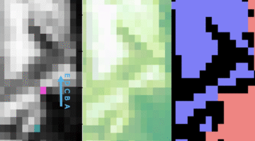
Machine learning tools and experiments at the ALS enabled the identification of defect-rich regions in single-crystalline Co3Sn2S2 that link to how surface electrons move. Atom-level understanding of how the surface electronic properties of a magnetic semimetal can be tuned could guide its use in advanced technologies like spintronics and catalysis. Read more »![]()
ALS Work Using ARPES
Angle-resolved photoemission spectroscopy (ARPES) is a technique in which a highly focused beam of x-rays is used to kick electrons out of the sample. By analyzing the ejected electrons' direction and energy, the researchers can obtain the material's band structure—a map of the electrons' behavior in the material.
Altermagnetism All the Way Down
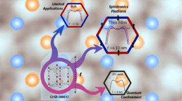
Altermagnets are an emerging class of magnetic materials that offer the potential for energy-efficient, high-density memory chips. Researchers at Penn State, UC Santa Barbara, and the ALS demonstrated that characteristic altermagnetic band splitting in chromium antimonide is evident in thin films relevant for real-world device application. Read more »
Separating an Electron into Waves of Spin and Charge
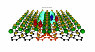
Researchers are exploring how a thin film can host a Tomonaga–Luttinger liquid, which separates an electron’s charge and spin. The research findings could contribute to the development of ultra-compact and energy-efficient technologies. Read more »
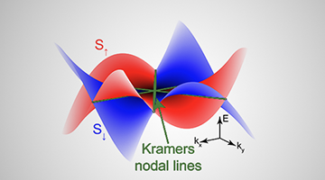
The Quest for an Altermagnet
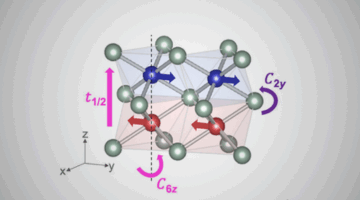
Researchers determine the unique electronic structure of altermagnets, which offers numerous benefits in creating energy-efficient devices based on spin-polarized electron currents. Understanding how altermagnetism works could contribute to the development of next-generation memory, logic, or sensing devices that are faster and consume less power. Read more »
Designing Quantum Materials for Future Electronics
Researchers bring theory into practice and confirm a new material’s characteristics at the ALS. The study opens new opportunities to design a substance that renders extra “handles” on the electron—not just its charge, but its spin and valley—so we can build computers that are faster, cooler, and more energy-efficient compared to traditional electronics. Read more »
Pinpointing Magnetic Mysteries and Mechanisms in a Layered Perovskite
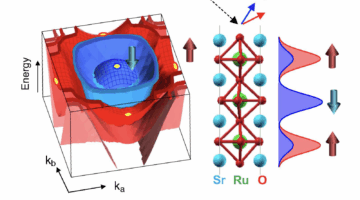
The strontium ruthenate family has a perovskite-like structure that can assemble into different configurations, offering an ideal way to study how the physics change as the material goes from 3D to 2D. In this study, researchers revealed how electrons with different spins behave in distinct layers of a three-layer magnetic material. The results deepen the field’s understanding of how magnetism emerges in layered materials, an important concept for future magnetic technologies and quantum electronic devices. Read more »![]()
![]()
A New Twist for Superconductivity in Bilayer Graphene

In a study of twisted bilayer graphene (TBG) systems, researchers found intriguing spectroscopic features in a superconducting “magic-angle” TBG—features that are absent in non-superconducting TBG. The results provide crucial information on superconductivity in magic-angle TBG for next-gen electronics and advanced energy technologies. Read more »![]()
![]()
Mapping the Quantum Landscape of Electrons in Solids
Researchers found a way to reconstruct quantum geometric tensors (QGTs)—mathematical entities that encode how an electron’s wave function is shaped by its quantum environment. The mapping of QGTs enables the discovery and control of novel quantum phenomena such as superconductivity and unconventional electronic phases. Read more »![]()
![]()
Hide-and-Seek with Sneaky Electrons in Solids
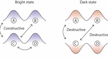
Researchers used angle-resolved photoemission spectroscopy (ARPES) at the Advanced Light Source (ALS) to demonstrate the existence of dark—state electrons in solids for the first time, providing insights into complex phenomena in physics, such as high-temperature superconductivity and optoelectronics.
Read more »
Not All Gaps Are Created Equal
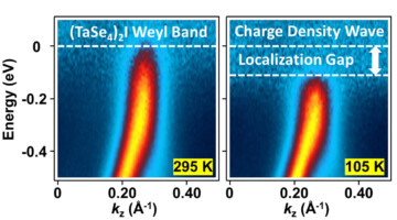
Researchers found that charge density waves (CDWs) in topological materials induce unconventional spectral gaps in the materials’ electronic structure. The finding that CDWs in topological materials can be essentially different from those in other materials should be carefully considered when designing quantum devices. Read more »![]()
- 1
- 2
- 3
- …
- 8
- Next Page »