Tungsten disulfide (WS2) is a model 2D material that exhibits special properties because of its atomic thinness. Such materials provide platforms for exploring fundamental quantum phenomena and applications in electronics, optics, or catalysis. Compared to bulk materials, 2D materials have electronic and optical properties that are more susceptible to defects, providing a way to create functional properties through defect engineering. While scientists have known about the presence of edge defects in WS2 flakes (a consequence of the sample growth process), their effects on material performance hadn’t previously been studied in a comprehensive and detailed way.
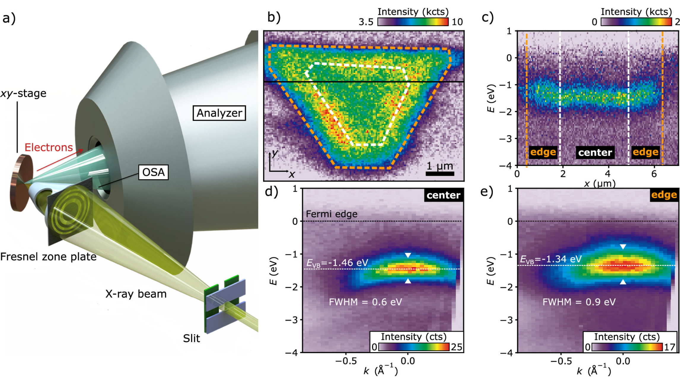
In this work, researchers studied WS2 using several techniques available at Berkeley Lab’s Advanced Light Source (ALS) and Molecular Foundry. Notably, it’s the first comprehensive study involving nanoscale angle-resolved photoemission spectroscopy (nanoARPES) at ALS Beamline 7.0.2, known as MAESTRO (Microscopic and Electronic Structure Observatory).
The overall results revealed that the sample edge regions had fewer sulfur atoms and more freely moving charge carriers than the center regions. With nanoARPES, the researchers found that the sulfur deficiency introduces a broadening and upward shift of the valence band. The broadening points to increased disorder in the edge region due to defects, which in turn may explain the upward shift of the valence band and the increased charge-carrier density. In future studies, the researchers plan to focus on induced defects, with the goal of controlling the amount and kinds of atoms that are affected and the locations where these defects are concentrated.

C. Kastl, R.J. Koch, C.T. Chen, J. Eichhorn, S. Ulstrup, A. Bostwick, C. Jozwiak, T.R. Kuykendall, N.J. Borys, F.M. Toma, S. Aloni, A. Weber-Bargioni, E. Rotenberg, and A.M. Schwartzberg, “Effects of Defects on Band Structure and Excitons in WS2 Revealed by Nanoscale Photoemission Spectroscopy,” ACS Nano 13, 1284 (2019), doi:10.1021/acsnano.8b06574.
Adapted from the Berkeley Lab news release, “Scientists Take a Deep Dive Into the Imperfect World of 2D Materials.”