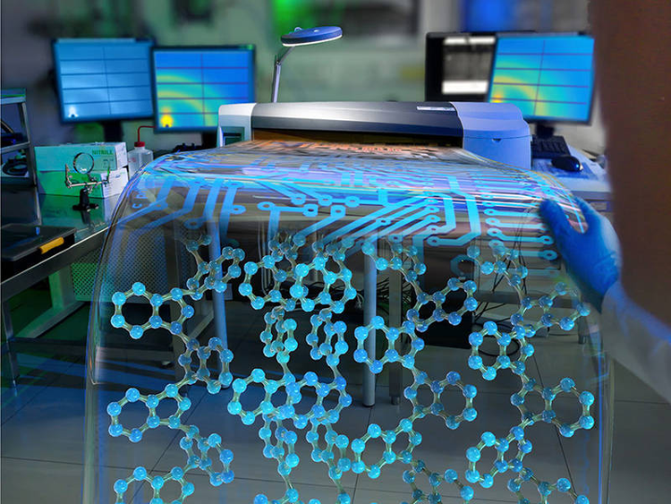
They are thin, light-weight, flexible, and can be produced cost- and energy-efficiently: printed microelectronic components made of synthetics. Flexible displays and touch screens, glowing films, RFID tags, and solar cells represent future markets.
An international team of researchers has now observed the creation of razor-thin polymer electrodes during the printing process and successfully improved the electrical properties of the printed films.
The x-rays were directed to the freshly printed synthetic layer and scattered. The arrangement and orientation of the molecules during the curing process of the printed films can be determined from changes in the scattering pattern.
Claudia M. Palumbiny, a scientist at the Technical University of Munich (TUM), investigated the “blocking layer” that sorts and selectively transports the charge carriers in the organic electronic components. Thanks to the intensive x-ray radiation and grazing-incidence wide-angle x-ray scattering (GIWAXS) methods used at Beamline 7.3.3, she and her colleagues achieved a very high time resolution, showing that even small changes in the physico-chemical processing conditions have a significant influence on the build-up and properties of the layer. Thus, the conductivity of the layer can be easily increased, and all layers could be produced using the same process, which would be a great advantage for manufacturers.

Work performed on ALS Beamline 7.3.3
Claudia M. Palumbiny, Feng Liu, Thomas P. Russell, Alexander Hexemer, Cheng Wang, and Peter Müller-Buschbaum “The Crystallization of PEDOT:PSS Polymeric Electrodes Probed In Situ during Printing” Advanced Materials 27, 3391 (2015).