Spin is a fundamental quantum property of electrons. This property takes on a new flair for topological insulators, materials whose interior prevents the free flow of electrical current but whose surface allows electrons to move easily. In these materials, electrons follow a different rule of the road—spin up electrons follow one path, while spin down electrons follow another. These rules define the distribution of electrons across the materials’ surface, which plays an important role in their exotic electronic properties and associated quantum phenomena.
To enhance these properties, researchers in the field of spintronics have been curious about the possibility of engineering an ideal material in which they can regulate electrons of opposite spins not only along the surface but also within the three-dimensional (3D) structure of the crystal. Controlling the movement of these electrons could produce desirable properties that may advance future applications in electronics and spintronics.
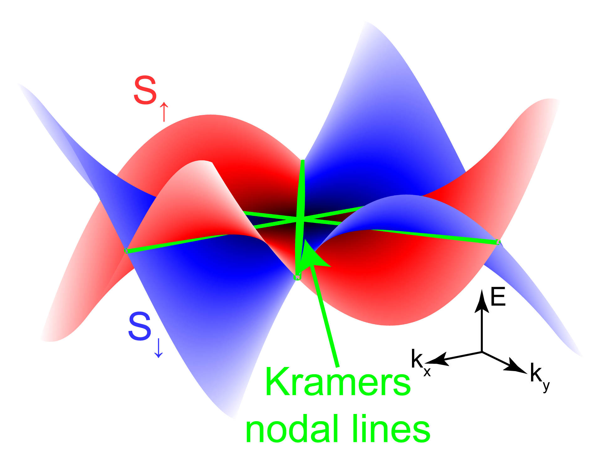
A team of researchers at Rice University led by Ming Yi and Emilia Morosan followed the theoretical predictions of Kramers nodal line (KNL) materials to engineer these ideal compounds. Their efforts generated a crystal composed of indium, tantalum, and sulfur (InxTaS2) where all the electrons follow the rules arising from an ideal KNL. The results of their study were published in the journal Nature Communications.
“This material came about by design following predictions on how a given crystal symmetry dictates a desired material property,” said Ming Yi, associate professor in physics and astronomy at Rice University and one of the senior authors on the paper. “Our team took a well-known 2D material and stuffed some intercalants in between the sheets to produce a material with the desired crystalline symmetries that locked in the special spin-dependent electron trajectories.”
Leveraging the electron superhighways
In quantum materials, electrons act like waves, and these waves can combine and cancel out in curious patterns. Sometimes, they get “stuck” along the KNLs, special paths where their energy levels meet and where the spin-up and spin-down electrons are yoked due to the symmetries of the crystal structure. The team found that by inserting indium into the crystal structure of certain well-known two-dimensional materials, they were able to change the crystalline symmetries and create such special pathways for the electrons.
“This is not trivial,” said Yichen Zhang, a doctoral student at Rice and co-first author on the study. “Our experiments indicate that we can precisely adjust the material’s properties to accentuate its topological traits, which is vital for future applications.”
The team brought their sample to Beamline 10.0.1 at the Advanced Light Source (ALS) and used spin-resolved angle-resolved photoemission spectroscopy (ARPES) to test their predictions. The beamline is equipped with 3D very-low-energy electron diffraction (VLEED) spin detectors, enabling the collection of electrons with different spin components. At the beamline, they measured the energy, momentum and spin of the electrons to demonstrate the presence of the predicted KNLs.
“With the development of new materials, we see more interest in this technique, and the ALS is committed to investing in this approach,” said Alexei Fedorov, a beamline scientist at 10.0.1. “As we modernize the MERLIN (4.0.3) beamline with the ALS upgrade, this technique will benefit from the additional capability to probe the spin texture in materials with a choice of different light polarizations and enable insights based on photoemission selection rules that users can explore.”
Yi and her team compared their experimental observations from the ALS with sophisticated first-principles theoretical calculations. The theoretical predictions aligned with the experimental data, providing deeper insights into the material’s electronic topology.
Bringing an idea to fruition
This new materials demonstrate superconductivity, the ability to carry electricity without energy loss. The results open new opportunities to create substances that can optimize quantum computers to enhance computation speed.
This work is based on a large family of versatile two-dimensional materials that is known for tunable properties by chemical substitution, intercalation, exfoliation, and strain. This work now adds the capability to tune the crystal properties for KNLs and superconductivity. The broad choice of elements may yield greater options for different applications and provide economic flexibility for industry to explore.
“Our work not only provides a realistic platform for realizing and tuning KNLs in layered materials but also paves the way for exploring the interplay between KNLs and superconductivity,” said Yi. “[It] provides a clear path for discovering and designing new quantum materials with desirable properties for future electronics.”

Zhang, Y., Gao, Y., Pulkkinen, A. et al. Kramers nodal lines in intercalated TaS2 superconductors. Nat Commun, 16, 4984 (2025). https://doi.org/10.1038/s41467-025-60020-z.