SCIENTIFIC ACHIEVEMENT
Researchers have successfully switched a topological insulator on and off by applying an electrical field.
SIGNIFICANCE AND IMPACT
The work represents a major advancement toward the creation of a functioning topological transistor that would allow devices to operate more efficiently at lower power than conventional electronics.

Switching to ultralow energy
A significant proportion of the growing amount of energy used in information and communications technology—such as mobile phones, computers, and the data centers that connect them—is caused by transistor switching. Each time a transistor switches, a tiny amount of energy is wasted as heat. With billions of transistors in each electronic device, switching billions of times each second, the amount of wasted energy adds up. In addition, continual progress in packing more transistors into smaller devices is pushing toward the physical limits of conventional materials, and researchers are in hot pursuit of alternatives that will allow devices to operate more efficiently at lower power. “Topological” materials are a promising solution, with the potential to drive the continued advancement of computing technology while at the same time minimizing power consumption.
Topological transistors
Topological insulators are novel materials that behave as electrical insulators in their interior but carry a current along their edges. In these edge paths, electrons can only travel in one direction: there can be no “back-scattering,” which is what causes the electrical resistance that generates waste heat. These properties can exist at room temperature (unlike in superconductors) and can persist even when the materials have structural defects and are subject to stress. But to be viable for current silicon-based technology, transistors made using topological insulators must also be able to switch rapidly between conducting and insulating states, modulated by an electrical signal.
In situ sample growth
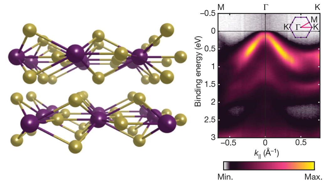
Sodium bismuthide (Na3Bi) is one of two materials known to be a “topological Dirac semimetal,” meaning it has unique electronic properties that can be tuned to behave in different ways—in some cases more like a conventional material and in other cases more like a topological material. Its topological properties were first confirmed in earlier experiments at the ALS.
In this work, the research team used molecular-beam epitaxy at ALS Beamline 10.0.1 to grow monolayer and bilayer Na3Bi samples on a silicon wafer. The sample-preparation capabilities at this beamline allow researchers to grow samples and then conduct experiments under the same vacuum conditions, preventing contamination.
Electric fields modify band structure
The researchers used angle-resolved photoemission spectroscopy (ARPES) at Beamline 10.0.1 to directly measure the material’s band gap, which determines whether or not the material is a conductor. To generate electric fields, they deposited varying amounts of potassium (K) on the sample surface. The potassium donates electrons to the material, leaving K+ ions behind on the surface. This is equivalent to a parallel-plate capacitor that generates an electric field that increases with the level of K dosing. The data showed a significant reduction in the band gap with increasing electric field.

To further clarify the effect, the researchers also measured the material’s response to the electric field generated by the close approach of a scanning tunneling microscope tip. The combined results verify that Na3Bi can indeed switch between conducting and insulating states under the influence of an electric field, offering the potential to support dissipationless current at room temperature in future transistor applications. The research team is now pursuing other samples that can be switched on and off in a similar way, to guide the development of a new generation of ultralow-energy electronics.

Contact: Mark T. Edmonds
Researchers: J.L. Collins, C. Liu, M.S. Fuhrer, and M. T. Edmonds (Monash University); A. Tadich (Monash University and Australian Synchrotron); W. Wu (Singapore University of Technology and Design); L.C. Gomes and J.N.B. Rodrigues (National University of Singapore and University of Illinois at Urbana-Champaign); J. Hellerstedt (Monash University and Institute of Physics of the Czech Academy of Sciences); H. Ryu (Korea Institute of Science and Technology and ALS); S.J. Tang and S.-K. Mo (ALS); S. Adam (National University of Singapore and Yale-NUS College, Singapore); and S.A. Yang (Singapore University of Technology and Design and Nanjing Normal University).
Funding: Australian Research Council, Australian Nuclear Science and Technology Organisation, Monash University, Singapore Ministry of Education, National University of Singapore, and National Supercomputing Centre, Singapore. Operation of the ALS is supported by the U.S. Department of Energy, Office of Science, Basic Energy Sciences Program (DOE BES).
Publication: J.L. Collins, A. Tadich, W. Wu, L.C. Gomes, J.N.B. Rodrigues, C. Liu, J. Hellerstedt, H. Ryu, S.J. Tang, S.-K. Mo, S. Adam, S.A. Yang, M.S. Fuhrer, and M. T. Edmonds, “Electric field-tuned topological phase transition in ultrathin Na3Bi,” Nature 564, 390 (2018), doi:10.1038/s41586-018-0788-5.
Adapted from the Monash University news release, “Ultra-low energy devices at the flick of a switch,” and the Berkeley Lab news release, “Topological Matters: Toward a New Kind of Transistor.”
ALS SCIENCE HIGHLIGHT #389