Electronic widgets (phones, computers, etc.) are getting better all the time, in size, speed, and power. However, it’s becoming harder to sustain this rate of improvement going forward because we’ve hit the limits of the materials that make up these devices.
“The only way we can continue the upward slog of ever-superior widget performance is to understand and engineer new materials that are the foundation of devices,” said Joshua Robinson, professor of Materials Science and Engineering at Penn State University.
To this end, Robinson led a group of researchers in exploring why graphene makes a good replacement for traditional metal contacts in junctions with transition metal dichalcogenides—a class of 2D semiconductors with advantageous electronic properties. The team’s findings were reported in the journal ACS Nano.
“Ohmic contacts are a critical part of advancing high-performance technologies—it’s the main junction where you get electricity in and out of a transistor,” said Robinson. “Historically, it’s been very hard to make good contacts to 2D semiconductors.”
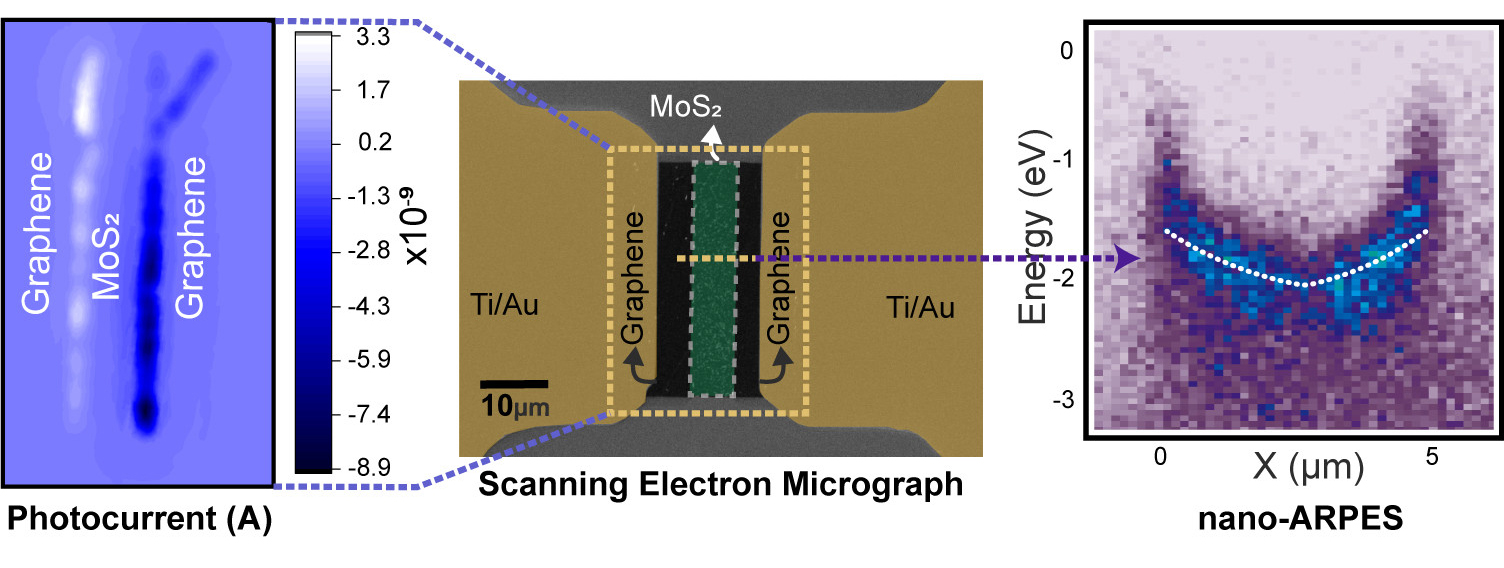
The group compared the performance of graphene to that of a traditional metal junction (Ti/Au) in contact with a 2D semiconductor, MoS2. They found that graphene performed ten times better than metal in transmitting a photoinduced current.
To better understand the transfer of charge across this interface, the researchers probed the spatial variation of the MoS2 band structure, utilizing the nanometer-scale resolution of the angle-resolved photoemission spectroscopy (nano-ARPES) system at ALS Beamline 7.0.2.
The results revealed that the valence-band maximum bends downward by about 500 meV, in agreement with theoretical calculations. The downward bending is a direct observation of a lowered potential-energy barrier (i.e., Schottky barrier) for electrons crossing the interface.
The work makes clear that, while interfaces between metals and 2D materials can be highly nonuniform, it may be possible to enhance performance by using graphene as a contact intermediary. More generally, a comprehensive understanding of charge transfer, gained through studies such as this, will help in engineering more efficient charge transport across microscopic interfaces.

S. Subramanian, Q.T. Campbell, S.K. Moser, J. Kiemle, P. Zimmermann, P. Seifert, F. Sigger, D. Sharma, H. Al-Sadeg, M. Labella, III, D. Waters, R.M. Feenstra, R.J. Koch, C. Jozwiak, A. Bostwick, E. Rotenberg, I. Dabo, A.W. Holleitner, T.E. Beechem, U. Wurstbauer, and J.A. Robinson, “Photophysics and electronic structure of lateral graphene/MoS2 and Metal/MoS2 junctions,” ACS Nano 14, 16663 (2020), doi: 10.1021/acsnano.0c02527.