A new measurement technique developed at the ALS is helping guide the semiconductor industry in next-generation nanopatterning techniques. Directed self assembly (DSA) of block copolymers is an extremely promising strategy for high-volume, cost-effective semiconductor manufacturing at the nanoscale. Materials that self-assemble spontaneously form nanostructures down to the molecular scale, which would revolutionize semiconductor manufacturing, but the key limitation for incorporation into manufacturing is the inability of conventional metrology tools to characterize the structure of the block copolymer. National Institute of Standards and Technology (NIST) and ALS researchers, in collaboration with IBM, have developed a new method using resonant x-ray scattering that for the first time has measured the fine scale features of the buried structure of the block copolymer. These results allow the validation of DSA process simulations and aid researchers in process development.

“From an industrial standpoint, we talk about how hard it is to do nanotechnology, to make tiny 20-nanometer structures on the surface of a semiconductor chip, which then form transistors,” says Jed Pitera, a research staff member in science and technology at IBM Research—Almaden. “But it’s also really hard to do the metrology, to measure what you’ve made and find out whether what you’ve put down on the wafer is what you think it is.
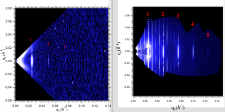
At ALS Beamline 11.0.1.2, NIST and IBM researchers developed a technique, resonant critical-dimension small-angle x-ray scattering (res-CDSAXS), that allows scientists to evaluate the 3D buried features inside a film. The ALS is currently the only place in the world that has such capability. The sample angle is varied to probe the 3D structure of the film, while resonant soft x-rays are used to enhance the scattering contrast. By measuring the same sample with both res-CDSAXS and traditional CDSAXS (with hard x-rays), the researchers were able to demonstrate the dramatic improvement in scattering obtained through the use of resonant soft x-rays.
Block copolymers are made by connecting two or more different polymers that form repeating shapes and patterns. The challenge is that the patterning has to be perfect, which makes measuring the full structure of the pattern important. The new ALS measurement technique reveals whether there is a poor match between the materials.
“Advances in metrology really drive our ability to do nanofabrication,” says Pitera. “Without the ALS, we don’t really have any non-destructive ways to see what’s going on in the interior of these materials.”

NIST materials scientist Joseph Kline explains that a key point of this development for industry users is that they will now be able to view structures under the surface of the block copolymers, rather than just the top layer that’s available to view with a traditional electron microscope. “Structures underneath the surface can be much more complicated,” says Kline. “We found this was true when we used this technique at the ALS.”
In addition to looking deep, researchers using the res-CDSAXS technique at the ALS are able to look at a large area of the sample, which IBM’s Pitera says is critical because they need self-assembly working perfectly across the entire silicon wafer.