SCIENTIFIC ACHIEVEMENT
Using a new method for stabilizing a two-dimensional (2D) metal on a large-area platform, researchers probed the origins of the material’s superconductivity at the Advanced Light Source (ALS).
SIGNIFICANCE AND IMPACT
The work represents a notable milestone in advancing 2D materials toward broad applications in topological computing, advanced optics, and molecular sensing.

Expanding the scientific palette
If you confine everyday metals to layers only a few atoms thick, they acquire new properties that are different from those exhibited by their more common bulk forms. The ability to synthesize such two-dimensional (2D) metals means that the range of materials available for novel uses can be expanded to different areas of the periodic table—providing a much richer “scientific palette” of properties for applications in topological computing, advanced optics, and molecular sensing.
Certain practical issues remain, however. Low-dimensional metals must be integrated into stable heterostructures at the wafer scale (currently up to about 15 cm in diameter). Also, metal surfaces exposed to air will oxidize (rust), and a 2D metal—essentially nothing but surface—would require protection from this kind of environmental degradation.
An atomic-layer sandwich
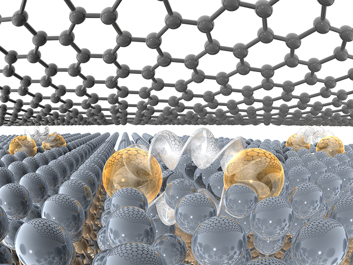
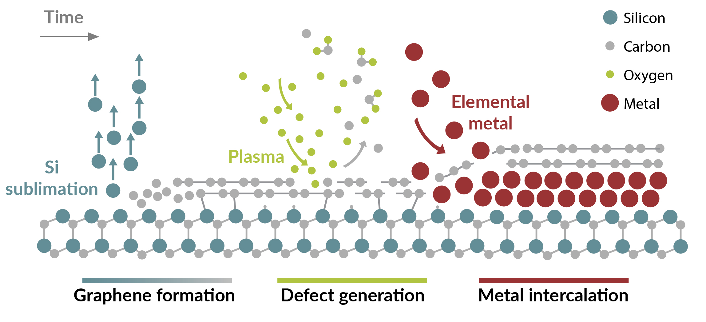
In earlier work, a team of researchers led by Joshua Robinson (Penn State University) developed a method to synthesize atomically thin, single-crystal layers of a semiconductor, sandwiched between a stable substrate of silicon carbide (SiC) and a protective top layer of epitaxial graphene. The method, dubbed confinement heteroepitaxy (CHet), starts by heating the SiC substrate to remove the top layers of silicon via sublimation. The surface carbon left behind re-forms into a layer of graphene, which is then exposed to oxygen plasma to generate defects. When pure metal powder is evaporated onto this surface, the metal atoms migrate through the defects in the graphene, which eventually heal at high temperatures.

With this process, the researchers were able to produce large-area, environmentally stable, single crystals of 2D gallium (Ga), indium (In), and tin (Sn). These metal atoms form “half van der Waals” layers—strongly bonded to the SiC substrate but weakly bonded to the graphene top layer. Competing synthesis methods are specific to certain metallic species and generally produce thicker layers without encapsulation, whereas CHet produces stable, atomically thin crystalline forms of diverse metals that do not otherwise exist in nature. The stability of these 2D metals in air over a period of months greatly facilitates ex situ characterization and enables facile processing and device fabrication.
Superconductivity in 2D gallium
Having shown that they could create novel crystalline systems at the interface of graphene and silicon carbide, the researchers began exploring what new properties in traditional materials may emerge. In this work, they focused on 2D Ga, demonstrating that it exhibits superconductivity with a higher transition temperature than its bulk counterpart.
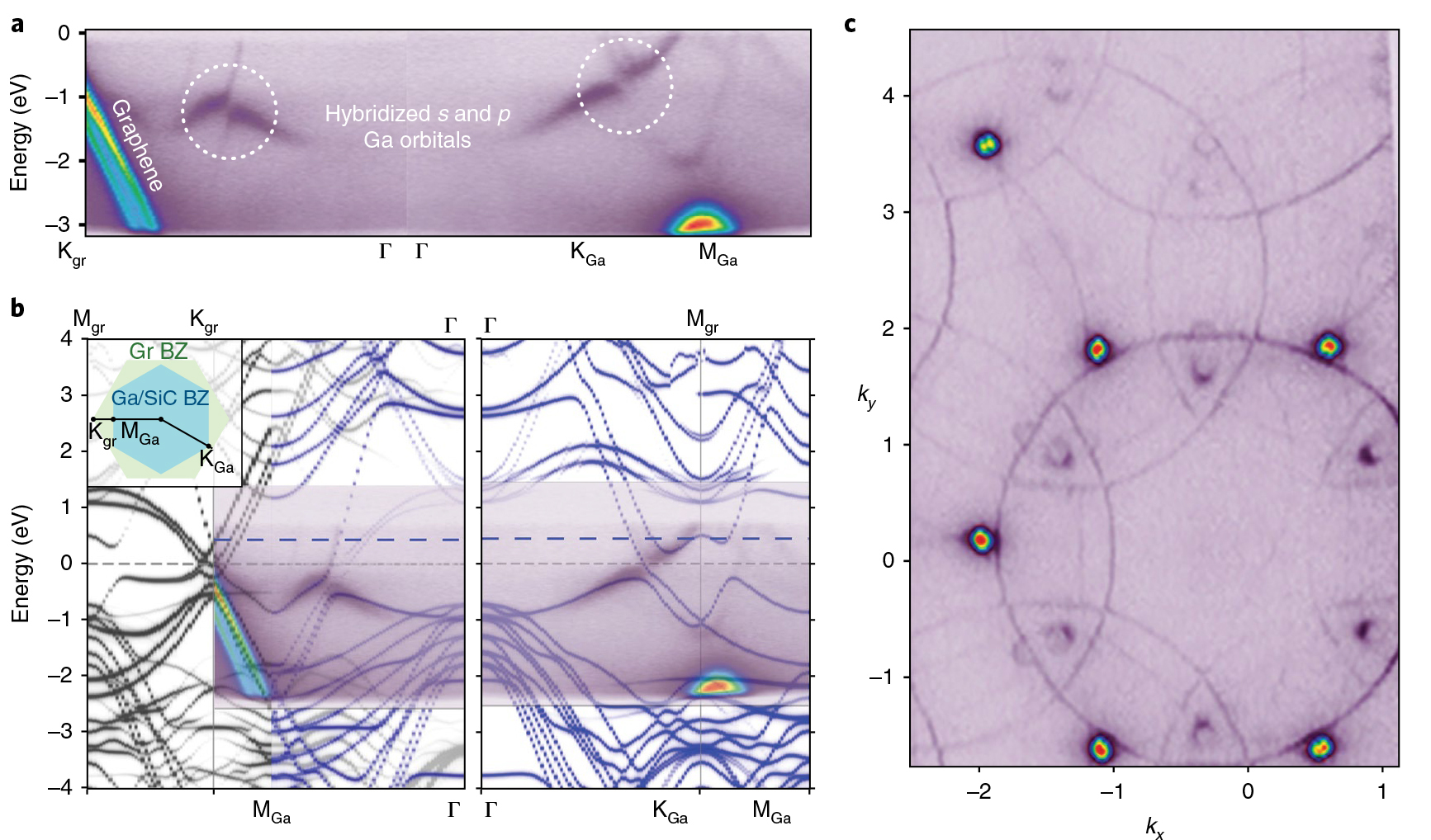
To gain a deeper understanding of the electronic behavior of this confined system, the researchers performed angle-resolved photoelectron spectroscopy (ARPES) experiments at ALS Beamline 7.0.2. Excellent agreement between the data and theoretical calculations confirmed the structural quality of the 2D Ga. The data also enabled the researchers to conclude that the observed superconductivity originates from the Ga, and not the graphene.
The work represents a notable milestone in the push toward realistic applications using 2D materials with technologically compelling properties. Future studies will focus on the origins of unique optical properties in these systems and on combining the emergent properties of 2D metals with other materials to form hybrid structures with engineered optical and quantum properties.

Contact: Joshua Robinson
Researchers: N. Briggs, B. Bersch, Y. Wang, J. Jiang, N. Nayir, K. Wang, A. De La Fuente Duran, S. Subramanian, C. Dong, J. Shallenberger, Y.-W. Chuang, C.-Z. Chang, J. Zhu, A.C.T. van Duin, V. Crespi, and J. Robinson (Pennsylvania State University); R.J. Koch (ALS and Berkeley Lab); M. Kolmer, W. Ko, M. Fu, Q. Zou, Z. Gai, and A.-P. Li (Oak Ridge National Laboratory); and A. Bostwick, C. Jozwiak, and E. Rotenberg (ALS).
Funding: Northrop Grumman, Semiconductor Research Corporation, Intel, National Science Foundation, Chinese Scholarship Council, and Alfred P. Sloan Foundation. Operation of the ALS is supported by the U.S. Department of Energy, Office of Science, Basic Energy Sciences program.
Publication: N. Briggs, B. Bersch, Y. Wang, J. Jiang, R.J. Koch, N. Nayir, K. Wang, M. Kolmer, W. Ko, A. De La Fuente Duran, S. Subramanian, C. Dong, J. Shallenberger, M. Fu, Q. Zou, Y.-W. Chuang, Z. Gai, A.-P. Li, A. Bostwick, C. Jozwiak, C.-Z. Chang, E. Rotenberg, J. Zhu, A.C.T. van Duin, V. Crespi, and J. Robinson, “Atomically thin half–van der Waals metals enabled by confinement heteroepitaxy,” Nat. Mater. 19, 637 (2020), doi:10.1038/s41563-020-0631-x.
ALS SCIENCE HIGHLIGHT #418