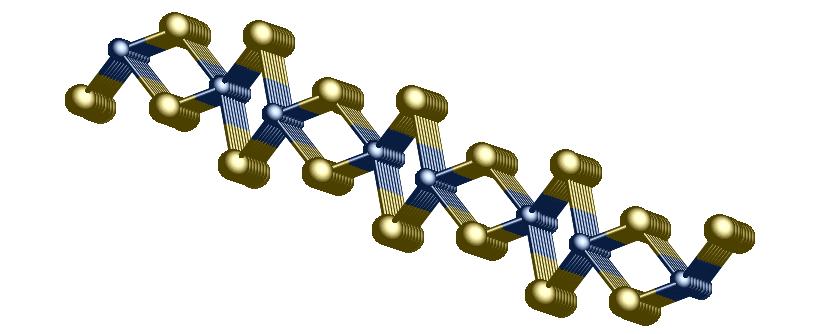
An international team of researchers fabricated an atomically thin layer of tungsten ditelluride (WTe2) and measured the exotic and durable properties that make it a promising candidate for spintronic applications. Angle-resolved photoemission spectroscopy (ARPES) at the ALS, combined with scanning tunneling microscopy (STM) experiments and first-principles calculations, have established that a particularly stable form of WTe2, the 1T′ structural phase (or “polytype”), is a two-dimensional topological insulator, confirming recent predictions. The findings should provide new opportunities for fundamental studies of topological phenomena and for next-generation spintronic applications.

The material under study, 1T′- WTe2, bridges two flourishing fields of research: that of so-called 2D materials, which include monolayer materials such as graphene that behave in different ways than their thicker forms, and topological materials, in which electrons can zip around in predictable ways with next to no resistance and regardless of the usual (nonmagnetic) defects that would ordinarily impede their movement. The material is called a topological insulator because its interior does not conduct electricity; its electrical conductivity is restricted to its edges. There, the direction in which the electrons flow is completely linked to the direction of their spins, a useful quality for spintronic devices. Such devices could conceivably carry data more fluidly, with lower power demands and less heat buildup than is typical in present-day electronic devices.
Three-atom-thick crystalline samples of the material were grown on a bilayer graphene substrate in a highly purified, vacuum-sealed compartment at the ALS, using molecular-beam epitaxy. The high-purity samples were then studied at Beamline 10.0.1 using ARPES, which provides a powerful probe of a material’s electronic properties. In the resulting data, the researchers immediately recognized two characteristic signatures of a 2D topological insulator: an inversion of the conduction and valence bands (caused by the 1T′ structural distortion) and a band-gap opening (caused by spin-orbit coupling).
Because the conducting part of the material, at its outermost edge, was only a few nanometers thick—thousands of times smaller than the x-ray beam’s focus—additional experiments using scanning tunneling microscopy (STM) were performed to measure the local density of electron states there. Comparison of the data obtained from the edges vs from the bulk showed a much higher conductance at the edges, as expected for a 2D topological insulator.
Two-dimensional materials have unique electronic properties that are considered key to adapting them for various applications, and there is a very active worldwide research and development effort focused on tailoring these materials for specific uses by selectively stacking different types. Researchers are trying to sandwich them on top of each other to tweak the material as they wish—like Lego blocks. Now, with experimental proof of this material’s properties, the goal is to stack it with other materials to see how these properties change.
A typical problem in creating such designer materials from atomically thin layers is that materials often have nanoscale defects that can be difficult to eliminate and that can affect their performance. But because 1T′-WTe2 is a topological insulator, its electronic properties are by nature resilient. At the nanoscale it may not be a perfect crystal, but the beauty of topological materials is that even when you have less-than-perfect crystals, the edge states survive. The imperfections don’t break the key properties.
Going forward, the researchers aim to develop larger samples of the material and to discover how to selectively tune and accentuate specific properties. Besides its topological properties, its “sister materials,” which have similar properties and were also studied by the research team, are known to be light-sensitive and have useful properties for solar cells and for optoelectronics, which control light for use in electronic devices.

Contacts: S.-K. Mo and Z.-X. Shen
Research conducted by: S. Tang (SLAC, Stanford, ALS, Chinese Academy of Sciences, and Shanghai Tech University); C. Zhang, C. Jia, H. Yan, R.G. Moore, T.P. Devereaux, and Z.-X. Shen (SLAC and Stanford); D. Wong, Z. Pedramrazi, H.-Z. Tsai, and S. Kahn (UC Berkeley); B. Moritz, M. Claassen, M. Hashimoto, and D. Lu (SLAC); H. Ryu (ALS; Pohang University of Science and Technology, Korea; and Pusan National University, Korea); J. Jiang (ALS, Shanghai Tech, and Pohang University); C.-C. Hwang (Pohang University); C. Hwang (Pusan National University); Z. Hussain and S.-K. Mo (ALS); Y. Chen (University of Oxford); M.M. Ugeda (Basque Foundation for Science, Spain, and CIC nanoGUNE, Spain); Z.Liu and X. Xie (Chinese Academy of Sciences and Shanghai Tech); and M.F. Crommie (UC Berkeley and Berkeley Lab).
Research funding: National Science Foundation; National Natural Science Foundation of China; China Postdoctoral Science Foundation; National Research Foundation of Korea; Spain Ministry of Economy and Competitiveness; and the U.S. Department of Energy, Office of Science, Basic Energy Sciences Program (DOE BES). Operation of the ALS is supported by DOE BES.
Publication about this research: S. Tang, C. Zhang, D. Wong, Z. Pedramrazi, H.-Z. Tsai, C. Jia, B. Moritz, M. Claassen, H. Ryu, S. Kahn, J. Jiang, H. Yan, M. Hashimoto, D. Lu, R.G. Moore, C.-C. Hwang, C. Hwang, Z. Hussain, Y. Chen, M.M. Ugeda, Z.Liu, X. Xie, T.P. Devereaux, M.F. Crommie, S.-K. Mo, and Z.-X. Shen, “Quantum spin Hall state in monolayer 1T′-WTe2,” Nat. Phys. 13, 683 (2017). doi:10.1038/nphys4174
Adapted from the Berkeley Lab news release, “2-D Material’s Traits Could Send Electronics R&D Spinning in New Directions.”
ALS SCIENCE HIGHLIGHT #361
