SCIENTIFIC ACHIEVEMENT
Using the Advanced Light Source (ALS), researchers found flat electronic band structures—known hallmarks of electrons trapped in two dimensions—but in a material that extends this phenomenon to three dimensions.
SIGNIFICANCE AND IMPACT
The work opens up a material framework for exploring superconductivity and other exotic states in three dimensions for advanced electronic applications.

A new dimension in exotic physics
When a material’s electrons are trapped together, they can settle into the same energy state and start to behave as one. In this collective state, the electron energies remain constant no matter what their momentum values are. In angle-resolved photoemission spectroscopy (ARPES) experiments, which map electron energy versus momentum, this state is signaled by a flat band in the data. Scientists predict that when electrons are in this state, they can start to feel the quantum effects of other electrons and act in coordinated, quantum ways. Then, exotic behavior such as superconductivity and unique forms of magnetism may emerge.
In this work, a team led by researchers from the Massachusetts Institute of Technology (MIT) have found a three-dimensional material that exhibits this distinctive flat-band signature in ARPES data, previously observed only for two-dimensional systems. With some chemical manipulation, the researchers also showed that they could transform the crystal into a superconductor—a material that conducts electricity with zero resistance.
Setting a 3D trap
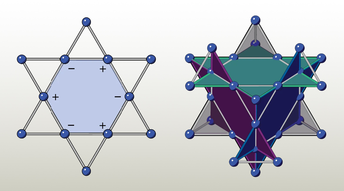
In work previously done at the ALS, the team observed that a two-dimensional lattice of interconnected, corner-sharing triangles (resembling Japanese “kagome” basket-weaving patterns) could confine electrons to the hexagonal space circumscribed by the triangles. But they and others also found that the electrons could escape up and out through the third dimension.
The team wondered: Could a three-dimensional configuration of similar lattices work to box in the electrons? In databases of material structures, they came across an atomic configuration associated with minerals known as pyrochlores. This structure forms a repeating pattern of cubes, with the face of each cube resembling a kagome-like lattice. The team found that, in theory, this geometry could effectively trap electrons within each cube.
Flat bands materialize
To test this hypothesis, the researchers synthesized a pyrochlore metal, CaNi2. Because the surface of this material is highly corrugated, photoemission studies of its electronic behavior require an ultrafocused beam of light capable of targeting specific locations across the uneven surface.
The sample was probed using vacuum ultraviolet (VUV) ARPES at ALS Beamline 7.0.2 (MAESTRO). Additional VUV and soft x-ray ARPES work was done at the National Synchrotron Light Source II (NSLS-II) and the Advanced Photon Source (APS), respectively. With the beamlines’ small spot sizes and ability to tune the photon energy, the researchers were able to directly observe extremely narrow bands in all three dimensions.
The data revealed three flat bands, at –0.41 ± 0.03 eV, –0.58 ± 0.03 eV, and –1.58 ± 0.05 eV. Theoretical models and further studies of electronic behavior using quantum oscillation measurements helped substantiate that the observed spectra are of bulk origin.
A glimpse at future possibilities
Finally, the researchers were able to chemically tune one of the flat bands by replacing the nickel in CaNi2 with a mixture of rhodium and ruthenium. This coincided with the appearance of superconductivity at a temperature of 6.2 K. From this point on, the researchers say, the challenge is to optimize flat-band materials to sustain superconductivity at higher temperatures. Such materials might someday enable ultra-efficient power lines, supercomputing quantum bits, and faster, smarter electronic devices.

Contacts: Riccardo Comin and Joseph Checkelsky
Researchers: J.P. Wakefield, P.M. Neves, D. Oh, S. Fang, R. McTigue, S.Y.F. Zhao, T.N. Lamichhane, A. Chen, M. Li, R. Comin, and J.G. Checkelsky (MIT); M. Kang (MIT and Max Planck POSTECH Center for Complex Phase Materials [Republic of Korea]; S. Lee, S. Park, and J.-H. Park (Max Planck POSTECH Center and Pohang University of Science and Technology); C. Jozwiak, A. Bostwick, and E. Rotenberg (ALS); A. Rajapitamahuni and E. Vescovo (NSLS-II); J.L. McChesney (APS); D. Graf (National High Magnetic Field Laboratory, Florida); J.C. Palmstrom (National High Magnetic Field Laborabory, New Mexico); and T. Suzuki (Toho University, Japan).
Funding: Gordon and Betty Moore Foundation; Air Force Office of Scientific Research; National Science Foundation; State of Florida; US Department of Energy (DOE), Office of Science, Basic Energy Sciences (BES) program, Center for Advancement of Topological Semimetals; National Research Foundation of Korea; Japan Society for the Promotion of Science. Operation of the ALS, NSLS-II, and APS is supported by DOE BES.
Publication: J.P. Wakefield, M. Kang, P.M. Neves, D. Oh, S. Fang, R. McTigue, S.Y.F. Zhao, T.N. Lamichhane, A. Chen, S. Lee, S. Park, J.-H. Park, C. Jozwiak, A. Bostwick, E. Rotenberg, A. Rajapitamahuni, E. Vescovo, J.L. McChesney, D. Graf, J.C. Palmstrom, T. Suzuki, M. Li, R. Comin, and J.G. Checkelsky, “Three-dimensional flat bands in pyrochlore metal CaNi2,” Nature 623, 301 (2023), doi:10.1038/s41586-023-06640-1.
Adapted from the MIT press release, “Physicists trap electrons in a 3D crystal for the first time.”
ALS SCIENCE HIGHLIGHT #496
| Read more about research on kagome materials at the ALS: |