SCIENTIFIC ACHIEVEMENT
Using several x-ray probes at the Advanced Light Source (ALS), researchers learned how the size, shape, and orientation of microstructures affect how they switch magnetization directions in response to an applied voltage.
SIGNIFICANCE AND IMPACT
The work advances our understanding of strain-responsive composite materials for use in energy-efficient electronic applications such as memory devices, sensors, and actuators.

Beyond the current approach
Today’s memory and logic devices require large electric currents to flip magnetic domains that store binary data. Unfortunately, this current-driven approach results in significant energy losses through heating. A more energy-efficient alternative is to control magnetization using voltage, through the use of multiferroic heterostructures—that is, a ferromagnetic layer coupled to a ferroelectric substrate. One promising material for the ferromagnetic layer is an iron-gallium alloy (Fe-Ga, or galfenol), known for its large magnetostrictive effect: its magnetization can significantly change in response to mechanical strain.
Composite Fe-Ga/PMN-PT samples
In this work, researchers explored the magnetoelectric behavior of tiny epitaxial Fe-Ga structures on a piezoelectric (PMN-PT) substrate, using multiple synchrotron x-ray probes. Studying such structures at small scales is vital to understanding how to manipulate them using voltage, with significant implications for the development of energy-efficient applications such as memory devices, sensors, and actuators.

The microstructures were designed to have different sizes (1–6 µm), shapes (square and elliptical), and crystallographic orientations with respect to the PMN-PT. A subnanometer-thick iron seed layer was used to initiate well-ordered Fe-Ga crystal growth, and a platinum capping layer was deposited to prevent surface oxidation.
Previous studies on epitaxial Fe-Ga-based multiferroic heterostructures have demonstrated impressive voltage-driven magnetic reorientation capabilities, but they focused on either continuous thin films or large structures of epitaxial Fe-Ga—far from the small features required for real-world devices.
Multimodal ALS experiments
To visualize voltage-driven magnetic reorientation in the Fe-Ga microstructures, the researchers used photoemission electron microscopy (PEEM) at ALS Beamline 11.0.1.1, with x-ray magnetic circular dichroism (XMCD) as a contrast mechanism. This beamline provides the ability to apply a voltage across the sample during measurement—ideal for studying electrically driven magnetic responses—as well as the ability to thin the platinum capping layer to about 0.5 nm just before the measurement.
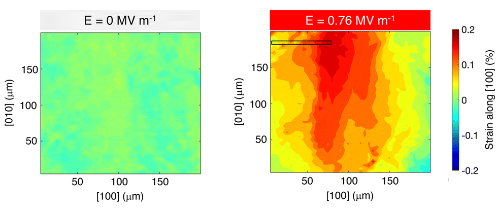
At ALS Beamline 12.3.2, the researchers used x-ray microdiffraction to measure micron-scale, voltage-induced strains in the piezoelectric substrate. The beamline’s integrated fluorescence mapping capability enabled the researchers to focus on the area right under the Fe-Ga microstructures, essential for correlating the local strains with the magnetic switching events observed using XMCD-PEEM.
Finally, at ALS Beamlines 4.0.2 and 6.3.1, x-ray magnetic spectroscopy was used to gain additional insight into the characteristics of the epitaxial Fe-Ga.
The shape of microstructure strain

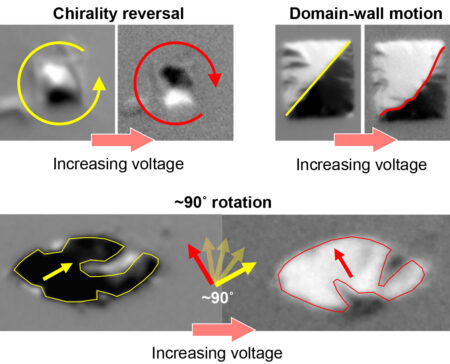
The XMCD-PEEM results revealed chirality reversal in 1 µm squares, domain-wall motion in 2 µm squares, and a ~90° rotation of the magnetization in the ellipses. Microdiffraction provided a quantitative map of the strain in the piezoelectric substrate, indicating a nonuniform, micron-scale strain distribution across the sample and the generation of a net tensile strain along one crystallographic axis. This information was vital to understanding the magnetic switching mechanisms of the Fe-Ga microstructures. The spectroscopy data showed that the iron was not oxidized, proving that a 0.5 nm thick platinum capping layer is sufficiently protective.
Overall, the work demonstrated that engineering the behavior of highly magnetostrictive epitaxial microdevices is possible and represents a vital step toward an energetically more efficient digital world.

Researchers: M. Goiriena (UC Berkeley and University of the Basque Country, UPV/EHU); Z. Xiao (UCLA and ALS); R. Steinhardt and D.G. Schlom (Cornell University); V. Estrada and A. Sepúlveda (UCLA); N. Tamura, R.V. Chopdekar, and A.T. N’Diaye (ALS); R.N. Candler (UCLA and California NanoSystems Institute); and J. Bokor (UC Berkeley and Berkeley Lab).
Funding: National Science Foundation, Ministry of Science and Innovation (Spain), and California NanoSystems Institute. Operation of the ALS is supported by the US Department of Energy, Office of Science, Basic Energy Sciences program.
Publication: M. Goiriena, Z. Xiao, R. Steinhardt, V. Estrada, N. Tamura, R.V. Chopdekar, A.T. N’Diaye, A. Sepúlveda, D.G. Schlom, R.N. Candler, and J. Bokor, “Imaging of voltage-controlled switching of magnetization in highly magnetostrictive epitaxial Fe–Ga microstructures,” Nanoscale 16, 9021 (2024), doi:10.1039/d4nr00739e.
ALS SCIENCE HIGHLIGHT #512