Electronic-structure studies showed that both infinitely light and infinitely massive particles coexist in a material with a star-shaped (kagome) crystal lattice. The material’s rich array of electronic behaviors shows promise for future spintronic applications and represents a new frontier for studying exotic phases of matter. Read more »![]()
![]()
ALS Work Using ARPES
Angle-resolved photoemission spectroscopy (ARPES) is a technique in which a highly focused beam of x-rays is used to kick electrons out of the sample. By analyzing the ejected electrons' direction and energy, the researchers can obtain the material's band structure—a map of the electrons' behavior in the material.
Chiral Crystals Give Rise to Topological Conductors
Researchers have discovered materials whose chiral crystal structures produce chirality in their electronic behavior. These topological conductors retain their unique electronic properties regardless of defects and open new possibilities in materials research. Read more »
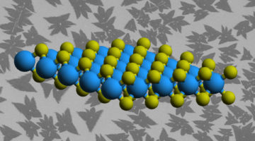
The Best Topological Conductor Yet: Spiraling Crystal Is the Key to Exotic Discovery
Researchers have discovered the strongest topological conductor yet, in the form of thin crystal samples that have a spiral-staircase structure. The realization of so-called topological materials—which exhibit exotic, defect-resistant properties and are expected to have applications in electronics, optics, quantum computing, and other fields—has opened up a new realm in materials discovery. Read more »
A Nanoscale View of Defect Effects on Band Structure
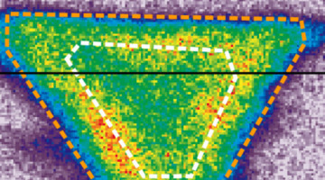
In the first comprehensive study at the ALS involving nanoARPES, researchers probed the electronic effects of defects in monolayer tungsten disulfide at the nanoscale. The extremely small scale of the measurements makes nanoARPES a great discovery tool that will be particularly useful for understanding new materials as they are invented. Read more »
Scientists Take a Deep Dive Into the Imperfect World of 2D Materials
Researchers combined a toolbox of techniques to home in on natural, nanoscale defects formed in the manufacture of monolayer WS2, measuring their electronic effects in detail not possible before. The latest result marks the first comprehensive study at the ALS involving nanoARPES, which researchers enlisted to probe the 2D samples with x-rays. Read more »
Spin-Momentum Locking in Cuprate High-Temperature Superconductors
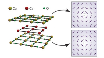
A form of spin-momentum locking, similar to the strong linkage between electron spin and momentum in topological insulators, has been found in a cuprate superconductor. The results open a new chapter in the mystery of high-temperature superconductors, suggesting that new, unexplored interactions and mechanisms might be at play. Read more »![]()
![]()
Electric-Field Switching of Topological Phase

Researchers have successfully switched a topological insulator on and off by applying an electrical field. The work represents a major advancement toward the creation of a functioning topological transistor that would allow devices to operate more efficiently at lower power than conventional electronics. Read more »![]()
![]()
The Electronic Structure of a “Kagome” Material
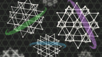
Scientists have verified exotic electronic properties predicted to emerge in a ferromagnetic material with “kagome” (trihexagonal) lattice symmetry. The greater understanding of kagome materials afforded by this work helps open up a new path toward goals such as ultralow-power electronic devices and quantum computing. Read more »![]()
![]()
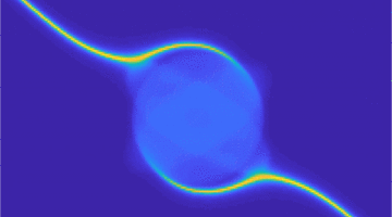
Tuning the Electronic Structure of a 2D Material
The electronic structure of a stacked 2D material was tuned by in situ electron doping, resulting in a large increase in the splitting of two valence bands. Stacked 2D materials possess an array of tunable properties that are expected to be important for future applications in electronics and optics. Read more »![]()
![]()
X-Ray Experiments Suggest High Tunability of 2D Material
Using the new MAESTRO platform at the ALS, scientists found that the exotic behavior of electrons in the 2D semiconductor, WS2, may be highly tunable, with possible applications for electronics and other forms of information storage, processing, and transfer. Read more »
- « Previous Page
- 1
- …
- 3
- 4
- 5
- 6
- 7
- 8
- Next Page »