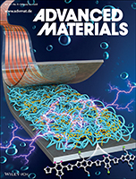
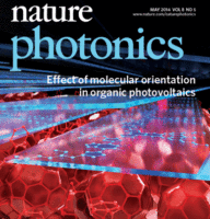
Realizing over 10% efficiency in printed organic solar cells via scalable materials and less toxic solvents remains a grand challenge. In this article, Harald Ade and co‐workers report chlorine‐free, in‐air blade‐coating of a new photoactive combination, FTAZ:IT‐M, which is able to yield an efficiency of nearly 11%, despite a high humidity of ≈50%. Read more »
Revealing the Blue Phase and Other Twisted Orders
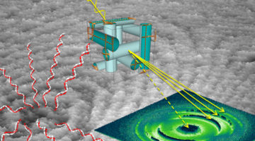
Resonant soft x-ray scattering revealed liquid crystal structures that cannot be probed using diffraction, including chiral liquid crystal systems such as the “blue phase” and the twist-bend nematic phase. Information on how individual molecules form functional structures in these systems is key to developing new applications. Read more »
Structure of Nanoscale-Pitch Helical Phases: Blue Phase and Twist-Bend Nematic Phase Resolved by Resonant Soft X-Ray Scattering
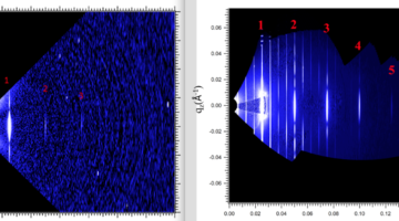
Resonant soft x-ray scattering (RSoXS) at the carbon K-edge was used to probe periodic structures of phases with orientational molecular order but homogeneous electron density distribution. This approach can be applied to structures with periodicities below the optical wavelength, to which neither optical nor classical x-ray diffraction techniques are sensitive. Read more »
Multifunctional Catalyst Balances Stability and Efficiency
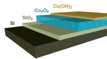
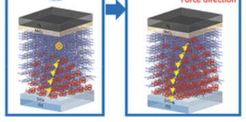
Scientists have found a way to engineer the atomic-scale chemical properties of a water-splitting catalyst for integration with a solar cell, and the result is a big boost to the stability and efficiency of artificial photosynthesis. Read more »![]()
![]()
Solar Cells Get Boost with Integration of Water-Splitting Catalyst onto Semiconductor
Scientists have found a way to engineer the atomic-scale chemical properties of a water-splitting catalyst for integration with a solar cell, and the result is a big boost to the stability and efficiency of artificial photosynthesis. Read more »
On the Way to Unlimited Energy
With the help of four different ALS beamlines, scientists were able to understand and improve the morphology of the main device structure in organic photovoltaic cells. Read more »![]()
Watching a Liquid-Crystal Helix Unwind
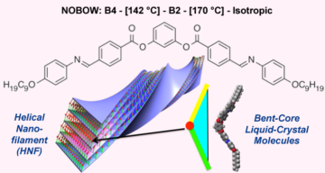
For the first time, researchers have directly measured the helical pitch of twisted liquid crystals composed of achiral bent-core molecules. The work opens the door to understanding the interplay between structure and property in important organic materials, including liquid crystals, lipid tubules, and peptoids. Read more »![]()
![]()
A Milky Mystery: The Case of the Casein Micelles
We all know that milk contains important nutrients such as calcium and protein that help build bones and muscle. But how much do we really know about these ingredients at the molecular level? To learn more, scientists from New Zealand and Australia came to the ALS to x-ray some milk.
Read more »
New ALS Technique Guides IBM in Next-Generation Semiconductor Development
A new measurement technique developed at the ALS is helping guide the semiconductor industry in next-generation nanopatterning techniques. NIST and IBM researchers collaborated on the technique, which allows scientists to evaluate the 3D buried features inside a film. The ALS is currently the only place in the world that has such capability.
The influence of molecular orientation on organic bulk heterojunction solar cells
Work done on ALS Beamlines 11.0.1.2, 7.3.3, and 5.3.2.2. reveals that preferential orientation of polymer chains with respect to the fullerene domain leads to a high photovoltaic performance. Read more »
