SCIENTIFIC ACHIEVEMENT
At the Advanced Light Source (ALS), researchers simultaneously monitored both the structure and function of a photovoltaic material as it crystallized from solution.
SIGNIFICANCE AND IMPACT
The work raises the prospect of rationally tuning materials for optimal performance in photovoltaics and other light-manipulating devices, including light-emitting diodes, detectors, and lasers.
Doctoral fellow Shambhavi Pratap summarizes her work on hybrid (organic–inorganic) perovskite solar-cell materials. (Credit: Marilyn Sargent/Berkeley Lab)
Next-generation photovoltaics
An exciting new solar material called organic–inorganic halide perovskites could one day help the U.S. achieve its solar ambitions and decarbonize the power grid. One thousand times thinner than silicon, perovskite solar materials can be tuned to respond to different colors of the solar spectrum simply by altering their composition mix.
Typically fabricated from organic molecules such as methylammonium and inorganic metal halides such as lead iodide, hybrid perovskite solar materials have a high tolerance for defects in their molecular structure and absorb visible light more efficiently than silicon. These qualities make perovskites promising active layers not only in photovoltaics, but also in other types of electronic devices that respond to or control light, including light-emitting diodes (LEDs), detectors, and lasers.
In search of hidden parameters
Despite their potential, perovskites have yet to be commercialized because the synthesis of stable, high-quality perovskite materials involves many nonequilibrium structures transforming into one another, greatly increasing the complexity of the process. Aside from many direct parameters that affect film formation, there are also hidden parameters that contribute to limited reproducibility and conflicting results.

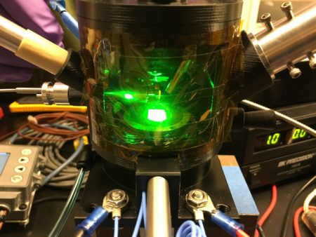
In this work, researchers described the synthesis of a metal halide perovskite, using grazing-incidence wide-angle x-ray scattering (GIWAXS) for structural information and laser-based photoluminescence spectroscopy for optical properties. A custom-made analytical chamber was developed at ALS Beamline 12.3.2 by Jonathan Slack, an ALS senior scientific engineering associate, Carolin Sutter-Fella, a scientist at Berkeley Lab’s Molecular Foundry, and former ALS doctoral fellow Shambhavi Pratap, who recently completed her doctoral studies in Peter Müller-Buschbaum’s group at the Technical University of Munich.
Multimodal studies at Beamline 12.3.2
The researchers studied the formation of thin films of methylammonium lead iodide (CH3NH3PbI3, or “MAPI”), the simplest perovskite to exhibit the desired photovoltaic properties. The synthesis process—spin coating, addition of antisolvent (solidifying agent), and annealing—was performed directly in the Beamline 12.3.2 hutch.
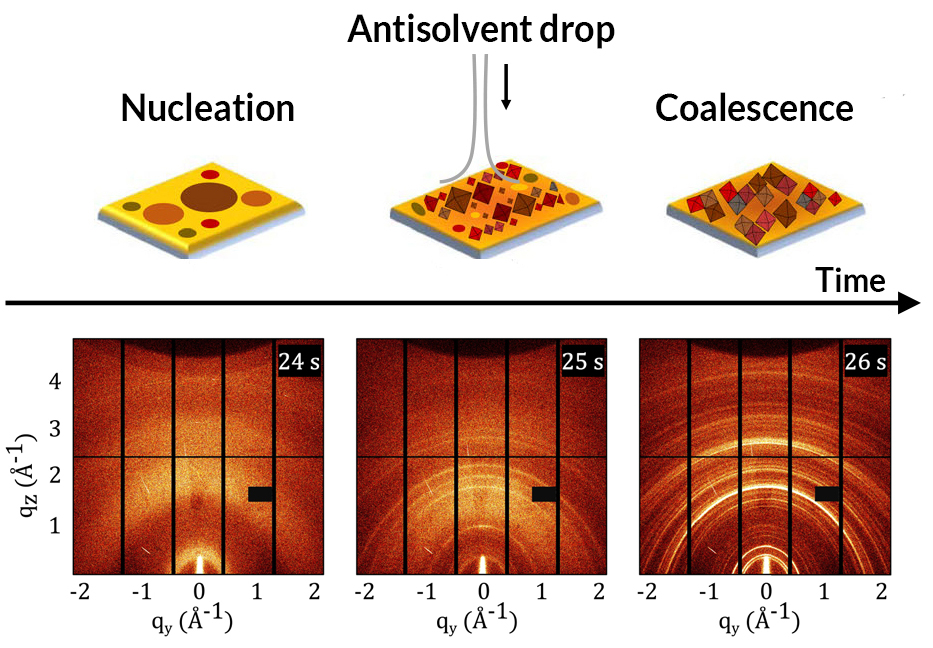
GIWAXS allowed the researchers to probe the material’s crystal structure in real time, for example in the moments just before and after a drop of antisolvent transforms the precursor solution. At the same time, laser-based photoluminescence spectroscopy was used to create electrons and holes in the perovskite, allowing observations of the material’s optical response.

Watching kinetics in real time

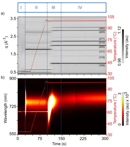
The evolution of MAPI was found to proceed in four steps: nanocrystal nucleation upon antisolvent drop, cluster coalescence, thermal decomposition upon solvent evaporation, and the formation of cubic crystals in thin film.
More crucially, the simultaneous scattering and spectroscopy data provided the researchers with complementary views of the crystallization kinetics, revealing how changes in optical response correlate with the evolution of the material structure. For example, immediately after the antisolvent drop, an intense and broad photoluminescence peak appeared, associated with the rapid formation of polydisperse (nonuniform) nanocrystals. Subsequent structural reorganizations offered similar clues as to the mechanisms underlying shifts in optical response.
Studies of more complex perovskites, planned for the future, raise the prospect of rationally tuning the materials for optimal photovoltaic performance, with simultaneous measurements becoming part of an automated workflow, monitoring the production of materials in real time for process and quality control.
Contacts: Peter Müller-Buschbaum and Carolin Sutter-Fella
Researchers: S. Pratap and P. Müller-Buschbaum (Technical University of Munich, Germany); F. Babbe, T. Luong, Z. Haber, T.-B. Song, and C.M. Sutter-Fella (Berkeley Lab); N.S. Barchi (Berkeley Lab and École Polytechnique Fédérale de Lausanne, Switzerland); Z. Yuan (Berkeley Lab and Pennsylvania State University); J.L. Slack and N. Tamura (ALS); and C.V. Stan (ALS and Lawrence Livermore National Laboratory).
Funding: Bavarian Collaborative Research Project Solar Technologies Go Hybrid (SolTech), German Research Foundation, TUM International Graduate School of Science and Engineering, Bavaria California Technology Center, Centre for Nanoscience (Munich, Germany), Nanosystems Initiative Munich, ALS Doctoral Fellowships in Residence, and Laboratory Directed Research and Development program at Berkeley Lab. Operation of the ALS is supported by the U.S. Department of Energy, Office of Science, Basic Energy Sciences program.
Publication: S. Pratap, F. Babbe, N.S. Barchi, Z. Yuan, T. Luong, Z. Haber, T.-B. Song, J.L. Slack, C.V. Stan, N. Tamura, C.M. Sutter-Fella, and P. Müller-Buschbaum, “Out-of-equilibrium processes in crystallization of organic-inorganic perovskites during spin coating,” Nat. Commun. 12, 5624 (2021), doi:10.1038/s41467-021-25898-5.
Adapted from the Berkeley Lab news release, “New Technique Paves the Way for Perfect Perovskites.”
ALS SCIENCE HIGHLIGHT #453